$D400-$D41C
54272-54273 $D400-$D401 FRELO1 FREHI1
Frequency control registers
The value in this pair of registers determines the frequency of the sound generated for voice 1. The higher the frequency, the higher the pitch of the sound. For triangle, sawtooth, and pulse waveforms, the relationship between the value in these registers and the voice 1 sound frequency in hertz (cycles per second) is:
frequency = register value * clock rate / 16777216
The first register (54272/$D400) holds the low byte of the value and the second (54273/$D401) holds the high byte. The clock rate depends on which video system the 128 uses. For NTSC (North American) systems, the clock value is 1022730 Hz, while for PAL (European) systems it is 985250 Hz. Thus, you can use the following expressions to calculate the frequency produced by any given register setting:
frequency = register value * 0.06096 (for NTSC systems)
frequency = register value * 0.05873 (for PAL systems)
Since the register pair can hold values from 0-65535/ $0000-$FFFF, the range of possible output frequencies for an NTSC system is 0-3995 Hz. A register value of zero corresponds to no frequency, hence no sound. The upper limit of human hearing is about 20,000 Hz, but the fact that the SID can’t generate frequencies above 4000 Hz isn’t really a serious handicap. The frequencies between 4000 and 20,000 Hz are not often used in music. For example, the highest note on a piano (a C four octaves above middle C) has a frequency of 4186 Hz, just slightly beyond the SID’s range. The SID can produce notes corresponding to those for any of the 88 keys on a piano keyboard except the very rightmost one. The lower limit of human hearing is about 20 Hz, so register values less than about 320/$0140 should result in inaudible output regardless of the volume setting. Actually, this is true only for the triangle waveform. The sudden transitions in output amplitude during sawtooth and pulse waveforms will produce a clicking or buzzing output at these supposedly inaudible low frequencies.
If you know the frequency (in hertz) that you wish to generate, you can calculate the corresponding register setting using the following formulae:
register value = desired frequency * 16.40 (for NTSC systems)
register value = desired frequency * 17.03 (for PAL systems)
It is permissible to change the frequency of a sound while it is playing. The change will take effect immediately, and will not affect the envelope. Changing the frequency of an active sound can produce interesting effects. See the entry for the register at 54299/$D41B for an example.
The noise waveform doesn’t have a regularly repeating pattern like the triangle, sawtooth, and pulse waveforms. The output jumps erratically from one amplitude level to another, so noise doesn’t really have a frequency in the same sense that the other waveforms do. For noise, the value in these registers determines how rapidly the amplitude level changes. The number of changes per second is approximately equal to the register value. For example, a register value of 1000/$03E8 will cause the noise output level to change about 1000 times per second, or approximately one change every 1/1000 second. The faster the output level changes, the higher the perceived pitch of the generated noise. Remember that these are write-only registers; they will always return 0/$00 when read, regardless of the values you have stored in them.
54274-54275 $D402-$D403 PWLO1 PWHI1
Pulsewidth control registers
This register pair controls the waveform shape when pulse output is selected for voice 1. The value here has no effect on any other waveform. The pulse waveform is binary; that is, it has two states: maximum amplitude and off (no amplitude). Unlike the ideal sine waveform, which has a smooth transition between maximum and minimum amplitudes, the pulse waveform switches almost instantly. The duration of each cycle of the waveform is controlled by the registers at 54272-54273/$D400-$D401. What the registers here control is how much of each cycle the waveform spends in the zero-amplitude state. Pulse waveforms are often described in terms of their duty cycles, the percentage of the total waveform cycle spent in the maximum amplitude state. A pulse waveform with a 0-percent duty cycle is always off, while a pulse waveform with a 100- percent duty cycle is always at maximum amplitude. A waveform with a 50-percent duty cycle is at maximum amplitude for half of the cycle and off for the remaining half, resulting in a square wave. Next figure illustrates various duty cycles.
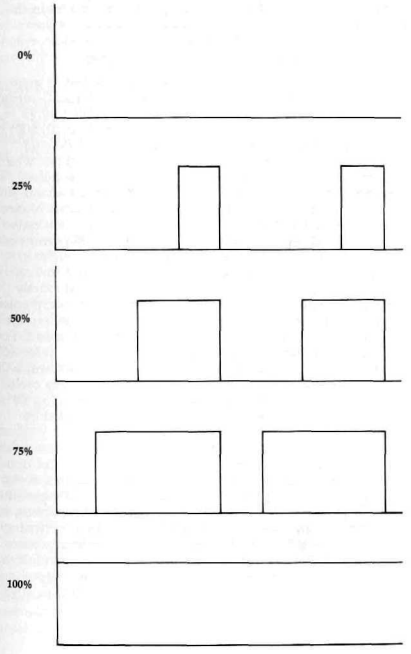
This register pair controls the duty cycle (expressed as a percentage of the total duration of one cycle of the waveform) according to the following formula:
duty cycle = 100 - (register value / 40.95)
Only 12 of the 16 bits in the register pair are used. The lower 8 bits come from the register at 54274/$D402 and the higher 4 bits come from bits 0-3 of the register at 54275/$D403. Bits 4-7 of 54275/$D403 are unused; any value written to these bits has no effect. The available 12 bits allow register values of 0-4095/$000-$EFF, Thus, you can specify duty cycles in the full range 0-100 percent. If you know the duty cycle you want, you can calculate the proper register value with: register value = (100 - desired duty cycle) * 40.95 In the expression above, the duty cycle is expressed as a percentage. For example, the required register value for a 50-percent duty cycle-a square wave-would be (100 - 50) * 40.95 = 2048/$0800. For this, you would store the low byte (0/$00) in 54274/$D402 and the high byte (8/$08) in 54275/$D403. There’s one phemomenon you need to be aware of when selecting duty cycles. The relative percentage of the pulse waveform cycle spent in each state, rather than the actual state, determines how the resulting output will sound. Notice in figure that both the 25-percent and 75-percent duty cycles have waveforms that are in one state for 25 percent of the cycle and the other state for 75 percent of the cycle. In either case, the ratio of time spent in each state is 3 to 1. A pulse wave with a 75-percent duty cycle will sound exactly the same as one with a 25-percent duty cycle. For every pulse waveform duty cycle less than 50 percent, there is a duty cycle greater than 50 percent that will produce the same sound. For example, a waveform with a 10-percent duty cycle (on for 10 percent of the cycle and off for the remaining 90 percent) will sound the same as a waveform with a 90-percent duty cycle (on for 90 percent of the cycle and off for the remaining 10 percent), since for either waveform the cycle is divided between the two states in a 9-to-1 ratio.
The closer the register value is to 2048/$0800-the value for a square wave (50-percent duty cycle, 1-to-1 ratio of time in each state)-the richer the resulting output will sound. As the register value approaches 4095 or 0, for 0- or 100-percent duty cycles, respectively, the ratio approaches its maximum of 1 to 4095 and the resulting sound output becomes increasingly thin. Very low or very high duty cycles result in nearly inaudible output. Duty cycles of exactly 0 or 100 percent result in constant output levels. Since some variation in the output is required to produce sound, register values of 0/$000 or 4095/ $FFFF produce no audible output. It is permissible to change the value in these registers, and hence the width of a pulse waveform, while the voice is generating output. This will affect only the waveform, not the envelope. Remember that these are write-only registers; they will always return 0/$00 when read, regardless of the values you have stored in them.
54276 $D404 VCREG1
Voice 1 control register
Each bit of this register controls some aspect of the output sound for the voice. Remember that this is a write-only register. All of the following bits return %0 when read.
Bit 0: this bit, called the gate flag, is used to initiate output for this voice and to trigger the release portion of the defined sound envelope for the voice. Writing a %1 here starts the attack portion of the envelope. This is sometimes referred to as gating the voice. For audible output, the frequency registers for this voice and the overall volume register for the chip must contain nonzero values. The attack portion of the envelope will normally be followed by the decay phase, after which the sound amplitude will remain at the specified sustain level until a %0 is written to this register. After the %0 is written, the release phase begins and the sound output level will fade away to silence at the specified release rate. Release does not occur unless a %0 is specifically written to this bit. Note that writing a %0 here triggers the release phase regardless of the current state of the envelope. For example, if you write a %1 here and then immediately write a %0 before the attack phase is completed, the attack will be aborted and release will begin from the current amplitude level. Likewise, writing a %1 here initiates the attack phase, regardless of the current state of the envelope. For example, if a %1 is written here while the envelope for the voice is in the decay phase, the decay phase will be aborted and another attack phase will begin from the current amplitude level.
Bit 1: this bit, called the sync flag, controls a special effect known as synchronization, which changes the frequency of and adds extra harmonics to the voice 1 output. When this bit is set to %1, the waveform of voice 1 will be synchronized with the waveform of voice 3. That is, whenever the waveform of voice 3 starts a new cycle, voice 1 will also start a new cycle, regardless of its point in its current waveform. Next figure illustrates the effect on the voice 1 waveform.
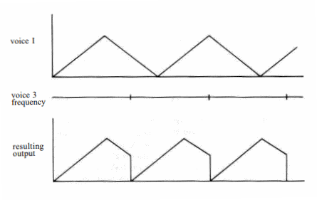
Only the frequency specified for voice 3 is significant for synchronization. In fact, it doesn’t matter whether voice 3 is turned on or not, so long as a frequency value is stored in the frequency control registers for the voice. Synchronization has no effect if the frequency for the synchronizing voice is zero. Ideally, the frequency for voice 3 should be less than that specified for voice 1. Synchronization also works for voices 2 and 3. Setting this bit in the control register for voice 2 (54283/$D40B) allows voice 2 to be synchronized with voice 1, and setting this bit in the control register for voice 3 (54290/$D412) allows voice 3 to be synchronized with voice 2. It is possible to have two or all three voices synchronized simultaneously.
Bit 2: this bit, called the ring mod flag, controls a special effect known as ring modulation. When this bit is set to %1 and a triangle waveform is selected for the voice, the triangle waveform will be ring modulated at the frequency of voice 3. Ring modulation works only when the triangle waveform is selected. Ring modulation is rather difficult to explain simply. When you ring modulate voice 1 at the frequency of voice 3, the resulting waveform is the equivalent to the sum of two waveforms of different frequencies. However, the resulting frequencies are different from both the frequency of voice 1 and that of voice 3. Next figure is an example of one observed ring-modulated output.
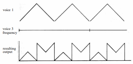
The ring modulated waveform will have a complex mix of harmonics. This is useful for simulating the sounds of bells, gongs, and similar instruments whose waveforms don’t closely resemble the triangle, sawtooth, or pulse. Only the frequency specified for voice 3 is significant for ring modulation. Voice 1 must be set for a triangle waveform, but the waveform of voice 3 is irrelevant. It doesn’t even matter whether voice 3 is turned on or not, as long as a frequency value is stored in the frequency control registers for the voice. Ring modulation has no audible effect if the frequency for the modulating voice is zero. Ring modulation also works for voices 2 and 3. Setting this bit in the control register for voice 2 (54283/$D40B) allows voice 2 to be ring modulated by voice 1. Voice 2 must be set for a triangle waveform. Setting this bit in the control register for voice 3 (54290/$D412) allows voice 3 to be ring modulated by voice 2. Voice 3 must be set for a triangle waveform. It is possible for two or all three voices to be simultaneously ring modulated.
Bit 3: this bit, called the test flag, can be used to reset the internal oscillator for the voice. When this bit is set to %1, the internal-oscillator register is reset to zero, halting sound output for the voice. The oscillator remains stopped until a %0 is written to this bit. You can use this bit to precisely control when the voice oscillator turns off or on. You must also use this bit to unfreeze the noise output if you accidentally turn on noise while another waveform is active.
Bits 4-7: these bits control the behavior of the internal oscillator for the voice, and hence the resulting waveform of the sound output for the voice. Each bit controls one of the standard waveforms, as follows:
| Bit | Value | Waveform |
|---|---|---|
| 4 | 16/$10 | triangle |
| 5 | 32/$20 | sawtooth |
| 6 | 64/$40 | pulse |
| 7 | 128/$80 | noise |
Setting one of these bits to %1 tells the oscillator to produce the corresponding waveform. Setting the bit to %0 turns off that waveform. One of the waveforms must be selected for the voice to produce any output.
Since the waveforms can be independently selected, you might be tempted to simultaneously enable more than one waveform for the voice. This won’t hurt the SID chip, but you’ll probably be disappointed with the results. When you select more than one waveform, the resulting output is not the simple combination of the selected waveforms. Commodore literature continues to claim that the result will be a logical ANDing of the selected waveforms, but the SID’s designer has stated that this is not the case. In any event, mixed waveforms tend to produce a rather erratic sound, so the technique isn’t really useful. Furthermore, you’ll cause a problem if one of the waveforms in the combination is noise. When the noise waveform is selected while any other waveform is also selected, the noise generator for the voice will cease to function. To restart it you’ll have to write a %1 and then a %0 to the TEST flag (bit 3 of this register) or reset the computer.
54277 $D405 ATDCY1
Attack and decay control register
This register controls the behavior of the attack and decay phases of the envelope for the voice.
Bits 0-3: these bits control the decay rate, the amount of time required for the voice to drop from the peak amplitude attained during the attack phase to the specified sustain level. For decay to have any audible effect, the sustain level must be less than %1111/$F. There is no simple formula relating the bit value to the corresponding time. The following table shows the relationship:
| Bits 3 2 1 0 | Value | Time required for decay phase (in seconds) |
|---|---|---|
| 0000 | 0/$00 | 0.006 |
| 0001 | 1/$01 | 0.024 |
| 0010 | 2/$02 | 0.048 |
| 0011 | 3/$03 | 0.072 |
| 0100 | 4/$04 | 0.114 |
| 0101 | 5/$05 | 0.168 |
| 0110 | 6/$06 | 0.204 |
| 0111 | 7/$07 | 0.240 |
| 1000 | 8/$08 | 0.300 |
| 1001 | 9/$09 | 0.750 |
| 1010 | 10/$0A | 1.5 |
| 1011 | 11/$0B | 2.4 |
| 1100 | 12/$0C | 3.0 |
| 1101 | 13/$0D | 9.0 |
| 1110 | 14/$0E | 15.0 |
| 1111 | 15/$0F | 24.0 |
You can change the decay rate while a sound is being played. However, unless the envelope is currently in the attack or decay phase, the change won’t have any effect until the next time the envelope is started by writing a %1 to the gate bit for the voice (bit 0 of the control register).
Bits 4-7: These bits control the attack rate, the amount of time required for the sound output of the voice to rise from silence (zero amplitude) to peak amplitude. The attack phase begins when a %1 is written to the gate bit for the voice (bit 0 of the control register). There is no simple formula relating bit values to the corresponding attack rates. The following table shows the relationship. Note that attack rates are three times faster than corresponding decay or release rates. This is because the attack phase tends to be shorter than decay or release for most naturally occurring sounds.
| Bits 7 6 5 4 | Value | Time required for attack phase (in seconds) |
|---|---|---|
| 0000 | 0/$00 | 0.002 |
| 0001 | 1/$01 | 0.008 |
| 0010 | 2/$02 | 0.016 |
| 0011 | 3/$03 | 0.024 |
| 0100 | 4/$04 | 0.038 |
| 0101 | 5/$05 | 0.056 |
| 0110 | 6/$06 | 0.068 |
| 0111 | 7/$07 | 0.080 |
| 1000 | 8/$08 | 0.100 |
| 1001 | 9/$09 | 0.250 |
| 1010 | 10/$0A | 0.5 |
| 1011 | 11/$0B | 0.8 |
| 1100 | 12/$0C | 1.0 |
| 1101 | 13/$0D | 3.0 |
| 1110 | 14/$0E | 5.0 |
| 1111 | 15/$0F | 8.0 |
You can change attack rate while a sound is being played. However, unless the envelope is currently in the attack phase, the change won’t have any effect until the next time the gate bit for the voice (bit 0 of the control register) is set to %1 to restart the envelope.
54278 $D406 SUREL1
Sustain and release control register
This register controls the behavior of the sustain and release phases of the envelope.
Bits 0-3: the value in these bits determines the amount of time required for the volume level for the voice to drop to zero (silence) during the release phase of the envelope. The release phase doesn’t begin until it is triggered by writing a %0 to bit 0 of the control register for the voice. Note that release will have no audible effect if the specified sustain level is zero. There’s no simple formula relating the value in these bits to the corresponding release times. The following table lists the relationships:
| Bits 3 2 1 0 | Value | Time required for release phase (in seconds) |
|---|---|---|
| 0000 | 0/$00 | 0.006 |
| 0001 | 1/$01 | 0.024 |
| 0010 | 2/$02 | 0.048 |
| 0011 | 3/$03 | 0.072 |
| 0100 | 4/$04 | 0.114 |
| 0101 | 5/$05 | 0.168 |
| 0110 | 6/$06 | 0.204 |
| 0111 | 7/$07 | 0.240 |
| 1000 | 8/$08 | 0.300 |
| 1001 | 9/$09 | 0.750 |
| 1010 | 10/$0A | 1.5 |
| 1011 | 11/$0B | 2.4 |
| 1100 | 12/$0C | 3.0 |
| 1101 | 13/$0D | 9.0 |
| 1110 | 14/$0E | 15.0 |
| 1111 | 15/$0F | 24.0 |
It is possible to change the release rate while a sound is being played. The new rate will supersede the old one, even if the envelope is currently in the release phase.
Bits 4-7: These registers specify the volume level at which the voice output will be maintained during the sustain level of the envelope. Note that this is different from the attack, decay, and release values, which specify periods of time instead of levels. Once the attack and decay phases are completed, the voice will remain at the level specified here until the release phase is specifically triggered by writing a %0 to the control register for the voice. The sustain level can be considered a percentage of the peak volume level of the output, as shown in the following table. The overall peak output level is controlled by bits 0-3 of the register at 54296/$D418. If 0 is specified for the sustain level, the voice will die away to silence at the end of the decay period. You can change the value in these bits to reduce the sustain level (and hence the output volume) while a sound is being played. However, if you try to increase the sustain level above its current value while a voice is in the sustain phase, the voice will be turned off.
| Bits 7 6 5 4 | Value | Percentage of peak output |
|---|---|---|
| 0000 | 0/$00 | 0 (no output) |
| 0001 | 1/$01 | 7 |
| 0010 | 2/$02 | 13 |
| 0011 | 3/$03 | 20 |
| 0100 | 4/$04 | 27 |
| 0101 | 5/$05 | 33 |
| 0110 | 6/$06 | 40 |
| 0111 | 7/$07 | 47 |
| 1000 | 8/$08 | 53 |
| 1001 | 9/$09 | 60 |
| 1010 | 10/$0A | 67 |
| 1011 | 11/$0B | 73 |
| 1100 | 12/$0C | 80 |
| 1101 | 13/$0D | 87 |
| 1110 | 14/$0E | 93 |
| 1111 | 15/$0F | 100 (peak output) |
Voice 2 Control Registers
The following seven registers (54279-54285/$D407-$D40D) provide the same control functions for voice 2 that the registers at 54272-54278/$D400-$D406 provide for voice 1. Refer to the entries for the voice 1 registers for details of how these registers are used.
54279 $D407 FRELO2
54280 $D408 FREHI2
Frequency control registers
54281 $D409 PWLO2
54282 $D40A PWHI2
Pulsewidth control registers
54283 $D40B VCREG2
Waveform control register
54284 $D40C ATDCY2
Attack and decay control register
54285 $D40D SUREL2
Sustain and release control register
Voice 3 Control Registers
The following seven registers (54286-54292/$D40E-$D414) provide the same control functions for voice 3 that the registers at 54272-54278/$D400-$D406 provide for voice 1. Refer to the entries for the voice 1 registers for details of how these registers are used.
54286 $D40E FRELO3
54287 $D40F FREHI3
Frequency control registers
54288 $D410 PWLO3
54289 $D411 PWHI3
Pulsewidth control registers
54290 $D412 VCREG3
Waveform control register
54291 $D413 ATDCY3
Attack and decay control register
54292 $D414 SUREL3
Sustain and release control register
54293-54294 $D415-$D416 FCLO-FCHI
Filter cutoff frequency registers
The value in these registers specifies the cutoff frequency for the filter. See the entry for bits 4-6 of the register at 54296/$D418 for more information on the effect of filtering. Only 11 of the 16 bits in this register pair are used. The lower 3 bits of the value come from bits 0-2 of the register at 54293/$D415 and the upper 8 bits come from the register at 54294/$D416. Bits 3-7 of 54293/$D415 are not used, and writing to those bits has no effect. Remember that these are write-only registers; they will always return 0/$00 when read, regardless of the values you have stored in them. The available 11 bits allow you to specify values in the range 0-2047/$0000-$07FF. However, there is a great deal of confusion about the exact relationship between the value in these registers and the corresponding cutoff frequency. Supposedly, the value here specifies the cutoff frequency in linear steps between a minimum of about 30 Hz and a maximum determined by two external capacitors connected to the SID chip. Commodore’s formal specifications for the SID chip state that the equation for maximum cutoff frequency is:
frequency = 2.6 X 10⁵ / capacitance
Other official literature, including the 128 Programmer’s Reference Guide, states that the maximum cutoff frequency is about 12,000 Hz, a calculation based on filtering capacitors of 2200 picofarads (2200 X 10-12). There are a number of problems here. First of all, the capacitors used in the 128 (and, by the way, also in later versions of the Commodore 64) are instead actually 470 picofarads, not 2200, If the stated equations were correct, this would give a maximum cutoff value of over 55,000 Hz, implying that the majority of register values would produce cutoff frequencies beyond the audible range. Simple experimentation shows that this is not the case. This isn’t surprising, since the SID’s designer, Bob Yannes, stated in an interview in the March 1985 issue of IEEE Spectrum magazine that filtering doesn’t work according to the specified equation anyway.
So how do you go about selecting a cutoff frequency? Our experience suggests that, while filtering does work after a fashion for any given 128, a value that produces a particular cutoff frequency on one computer may produce a slightly different cutoff frequency on another system. Although it’s not a particularly scientific approach, the best way to discover the proper register value for a given cutoff frequency is simply to try different values until the desired effect is achieved.
54295 $D417 RES/FILT
Filter selection and resonance control register
The bits of this chip select whether the various audio sources in the SID will be passed directly to the chip output or routed through the filter stage. This register also controls a special filtering effect known as resonance. Remember that this register is write-only; all bits will return %0 when read, regardless of the values you write to them.
Bit 0: this bit controls whether or not the output for voice 1 passes through the SID’s filter stage. When the bit is %0, the filter is bypassed and voice 1 output is routed directly to the combined SID output. When the bit is %1, voice 1 output is routed through the filter before being passed to the chip output. The filter will modify the voice 1 output according to the filter parameters specified in the registers at 54293-54294/$D415-$D416 and 54296/$D418.
Bit 1: this bit provides the same filter control function for voice 2 that bit 0 provides for voice 1.
Bit 2: this bit provides the same filter control function for voice 3 that bit 0 provides for voice 1.
Bit 3: this bit controls the handling of any external audio input to the SID. As with bits 0-3, setting this bit to %0 connects the external input directly to the combined output, while setting the bit to %1 routes the external input through the filter before output. These two functions-adding directly to the output or adding to the filtered output-are the only processing the SID can perform on the input signal from an external source. The SID’s external input line is connected to pin 5 of the composite (40-column) video port. To avoid damage to the SID, you should not use highly amplified signals such as the final output of a home stereo system for the external input source.
Bits 4-7: these bits control an effect of filtering known as resonance. The four bits provide for 16 evenly spaced steps from no resonance (%0000) to full resonance (%1111). Resonance accentuates frequencies near the cutoff frequency for the filter. The higher the resonance, the more pronounced the effect of the selected filter.
54296 $D418 SIGVOL
Volume and filter mode control register
This register controls the overall volume of the SID output, as well as the type of frequency attenuation provided by the filter. Remember that this register is write-only; reading any of the following bits will return %0, regardless of the values you write to the bits.
Bits 0-3: these bits specify the peak volume for the combined output of all three voices plus any external input. The four bits allow for 16 evenly spaced steps between no output (%0000) and maximum output (%1111). Expressed as a percentage of maximum possible output volume, the effects of the settings are roughly as follows:
| Bits 3 2 1 0 | Value | Percentage of maximum output |
|---|---|---|
| 0000 | 0/$00 | 0 (no output) |
| 0001 | 1/$01 | 7 |
| 0010 | 2/$02 | 13 |
| 0011 | 3/$03 | 20 |
| 0100 | 4/$04 | 27 |
| 0101 | 5/$05 | 33 |
| 0110 | 6/$06 | 40 |
| 0111 | 7/$07 | 47 |
| 1000 | 8/$08 | 53 |
| 1001 | 9/$09 | 60 |
| 1010 | 10/$0A | 67 |
| 1011 | 11/$0B | 73 |
| 1100 | 12/$0C | 80 |
| 1101 | 13/$0D | 87 |
| 1110 | 14/$0E | 93 |
| 1111 | 15/$0F | 100 (peak output) |
These bits must be set to some value greater than zero for the SID to produce any audible output. There’s only one volume control for the chip, but the relative output volume level of each voice can be controlled by adjusting the sustain level of the voice’s envelope.
Bits 4-6: these bits control the operation of the SID’s filter stage. The SID has only one filter for all three voices (plus the external input), so the filtering selections affect any source passed through the filter. Any of the voices can also bypass the filter and connect directly to the output. Bits 0-3 of the register at 54295/$D417 control which voices are routed through the filter. Bits 4-7 of that register control resonance, which can be used to emphasize the effects of filtering. The SID provides three basic types of filtering, as illustrated in next figure (a-c). The first type, called a low-pass filter, allows frequencies below a specified cutoff frequency to pass virtually unchanged, but sharply reduces (attenuates) the volume of frequencies higher than the cutoff.
The high-pass filter provides the opposite effect, allowing frequencies above the specified cutoff to pass while attenuating frequencies lower than the cutoff. The third selection, the band-pass filter, allows frequencies near the specified cutoff to pass while blocking frequencies that are much above or below the cutoff. The filtering types can also be combined. For example, selecting low-pass and high-pass filters simultaneously provides a fourth type of filter known as the band-stop, or notch, filter (next figure d). In this case, frequencies well above and below the cutoff are passed with little change, while frequencies near the cutoff are attenuated. The cutoff frequency is specified in the registers at $D415-$D416.
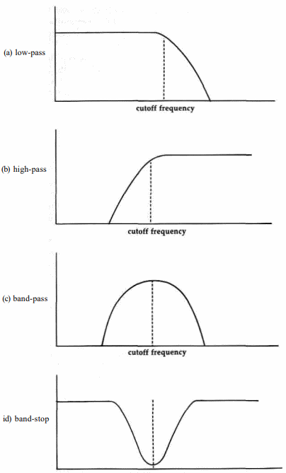
Bit 4 controls the low-pass filter, which is enabled when the bit is %1 and disabled when the bit is %0. Bits 5 and 6 provide the control for the high-pass and band-pass filters, respectively, in the same manner. Thus, standard filter selections are as follows:
| Bits 6 5 4 | Value | Filter type |
|---|---|---|
| 0 0 1 | 16/$10 | Low-pass |
| 0 1 0 | 32/$20 | Band-pass |
| 1 0 0 | 64/$40 | High-pass |
| 1 0 1 | 80/$50 | Band-stop |
Bit 7: this bit controls whether or not voice 3 can be connected directly to the combined output of the SID chip. While the bit is %0, the voice 3 output will be added to the combined output unless it is routed through the filter. Setting this bit to %1 will prevent the direct connection of voice 3 to the combined output. However, even when voice 3 is blocked from direct connection to the combined output, it’s still possible to route voice 3 output through the filter and hence to the combined output. To prevent this and completely disconnect voice 3, make sure that bit 2 of the register at 54295/$D417 is set to %0.
Voice 3 is often used in conjunction with one of the other voices to generate special audio effects, since the oscillator and envelope generator output values for this voice can be read from registers $D41B and $D41C, respectively. While voice 3 is used to generate special envelopes or as a random-number generator, it’s desirable to insure that the specified frequency and envelope for voice 3 don’t cause any disruption of the other voices. This bit provides that feature. Voice 3 is the only voice which can be disconnected.
54297-54298 $D419-$D41A POTX POTY
Potentiometer (paddle) reading registers
The SID chip has two special input lines, designated POTX and POTY, which are connected to a pair of internal devices called analog-to-digital (A/D) converters. The A/D converters generate a one-byte value based on the input voltage. These read-only registers return the values generated by the converters; writing to these locations has no effect. As connected in the 128, the converters measure the voltage across capacitors at the input pins. When a variable resistor (also called a potentiometer) is connected between a constant voltage source and the capacitor, the converters can be used to read the input resistance. The output values will be in the range 0-255, according to the resistor value. Minimum resistance (or a closed circuit) produces a reading of 0/$00 and maximum resistance (or an open circuit, as when nothing is connected to the lines) results in a reading of 255/$FF. The official SID chip specifications state that the relationship between the installed capacitor values and the resistance for maximum output value is:
resistor value = 4.7 X 10⁴ / capacitor value
The capacitors in the 128 are 1800 picofarads (1800 X 1012), so any resistance greater than about 4.7 X 10O4 / 1800 X IO-12 = 261 X 103 ohms (261 KΩ) will result in a register value of 255/$FF. Actually, our experience indicates that a slightly higher value, 270-280 KQ or so, may be required.
The SID input lines can be connected to either of the two control ports on the right side of the 128. Bits 6-7 of the CIA #1 port A register at $DC00 determine which control port is currently connected (for details, see the section on the CIA chip later in this chapter). The default setting connects control port 1, the front one. For either port, the SID register lines are connected to port pins 5 and 9. Location 54297/ $D419 will read the level at pin 9 and location 54298/$D41A will read the level at pin 5. From BASIC, the POT function can be used to read these registers. POT(l) reads the register at 54297/$D419 connected to pin 9 of port 1 and POT(2) reads the register at 54298/$D41A connected to pin 5 of port 1. POT(3) and POT(4) read the same registers when connected, respectively, to pins 9 and 5 of port 2.
The device most commonly connected to these inputs is the game paddle controller. A paddle is an extremely simple device, consisting of a variable resistor connected between a
- 5 volt source (pin 7 of the control port) and the SID A/D converter input line. Turning the paddle knob changes the resistance, and hence the register value. The paddle tends to be more efficient than the joystick for games that require only horizontal or only vertical movement, such as Pong-type games for which the paddle was originally developed. Since the steps between output levels are so small (only about one ohm), consecutive readings of the same paddle position can vary by one or two register values. This “jitter” can be annoying. The recommended solution is to read the paddle several times, then calculate the average of the readings and use that value.
One thing you should be aware of is that Commodore has changed the values of the capacitors used with the converters since the Commodore 64 was first introduced. The original 64 used 1000 picofarad capacitors, so a resistance of about 470 KX2 was required for a maximum register value. Thus, most paddles currently available for Commodore computers use potentiometers with a top resistance of 470 KΩ or 500 KΩ. Such paddles can be used with the 128, but they will swing the full range of register values (0-255) in about the first half of the paddle’s full turn. Thus, you probably won’t be able to select fine increments of intermediate values. Furthermore, paddles for Atari computers, which are much more widely available than Commodore paddles, use 1 MΩ (1 million ohm) potentiometers. Again, these can be used with the 128, but in this case you’ll see the full register value swing (0-255) in about the first quarter of the paddle’s full turn. Thus, Atari paddles will give you only very coarse control of the resulting register values. Most paddle controllers also have fire buttons like joysticks. However, since paddles almost always come in pairs, and since there is only one fire button line per control port, the paddle fire buttons are connected to the lines normally used for joystick direction. Standard Commodore paddles use the lines connected to bits 2 and 3 of each CIA #1 data port (locations $DC00-$DC01), the lines for joystick left and right.
These A/D converters can also be used for other interfacing projects. Any device which provides a variable resistance can be connected to the appropriate control port lines and read via these registers. For example, most graphics tablets such as the popular KoalaPad effectively function as paddles, with one resistance for the horizontal coordinate of the stylus position and another for the vertical coordinate. You could also rig an interface for an Apple/IBM-style joystick, which consists of two variable resistors-one on the horizontal axis and one on the vertical axis.
54299 $D41B OSC3
Voice 3 oscillator output register
This register reflects the upper eight bits of the internal-oscillator register for voice 3. This is a read-only register; storing values here has no effect. The output signal for each voice is generated by converting the digital bit pattern from the voice’s oscillator register into an analog voltage level, so the output signal for the voice is directly proportional to the value in its oscillator. However, voice 3 is the only voice for which the oscillator contents can be read. For triangle and sawtooth waveforms, the oscillator acts as a repeating counter. For the triangle waveform, the oscillator count starts at zero and increments upward to its maximum count, then decrements downward to zero again. Once the count reaches zero, it immediately begins incrementing again, and the process repeats over and over. The counting rate depends on the value in the frequency control registers for the voice. For all but the lowest frequencies, the count sweeps up and down so quickly that you won’t read every intermediate value between 0/$00 and 255/$FF in this register. For the sawtooth waveform, the count also starts at zero and increments upward to maximum count, but in this case the count then returns immediately to zero and begins incrementing again.
Unlike the triangle and sawtooth waveforms, the pulse waveform doesn’t sweep smoothly from one output level to the next. Instead, the it jumps back and forth between two discrete levels. When the pulse waveform is selected for voice 3, this register will contain one of two values: 0/$00 when the waveform is at minimum (zero) amplitude and 255/$FF when the waveform is at maximum amplitude. The portion of the cycle spent in the zero-amplitude state is determined by the value in the pulsewidth registers for the voice, and the rate at which the off/on switching repeats is determined by the value in the frequency control registers for the voice. The noise waveform is different from the others in that it exhibits no regularly repeating pattern. Rather, the oscillator will contain a series of random values. The rate at which the value in the oscillator changes-and hence the rate at which the value in this register changes-is determined by the value in the frequency control registers for the voice. This feature can be used to provide a random-number generator. If your program needs random numbers in the range 0-255/$00-$FF, simply set the voice 3 frequency registers ($D40E-$D40F) for a high frequency; then set bits 0 and 7 of the voice 3 control register ($D412) to %1 to start the noise waveform. After that, just read this register whenever you need a random value. In addition to its use as a random-number generator, this register can be used for a number of special audio effects. The changing output of the oscillator can be used to modify the frequency or pulsewidth of a voice or the filter parameters in realtime. The following is a simple example:
1B00 LDA #$F0 ;set sustain to maximum level
1B02 STA $D406
1B05 LDA #$8F ;set maximum volume; disconnect voice 3
1B07 STA $D418
1B0A LDA #$01 ;set frequency (high byte) for voice 3
1B0C STA $D40F
1B0F LDA #$21 ;start sawtooth waveform on voice 3
1B11 STA $D412
1B14 LDA #$11 ;start triangle waveform on voice 1
1B16 STA $D404
1B19 LDA $D41B ;change voice 1 frequency according to
1B1C STA $D401 ;voice 3 oscillator output
1B1F JMP $1B19
Whenever voice 3 is used for special effects such as random-number generation, it should be disconnected from the combined SID output so that it doesn’t distort any sounds produced by the other voices. To disconnect voice 3, set bit 7 to %1 in the register at $D418. Also, make sure that bit 2 of the register at $D417 is %0. This will insure that voice 3 output is not routed through the filter.
54300 $D41C ENV3
Envelope generator 3 output register
The value in this register reflects the contents of the internal envelope generator for voice 3, This is a read-only register; storing values here has no effect. Each voice has its own envelope generator which controls the peak amplitude of the output for that voice. However, voice 3 is the only one for which the envelope-generator register contents can be read.
The envelope generator regulates the amplitude (volume) of the output for the voice. When voice 3 is silent or turned off, this register will contain 0/$00, indicating no output. When the gate bit for the voice (bit 0 in the register at $D412) is set to %1, the value here will begin incrementing to 255/$FF, indicating peak output amplitude. This peak amplitude for the voice will be relative to the overall peak volume level specified in bits 0-3 of the register at 54296/$D418. The rate at which the register increments depends on the attack rate specified in bits 4-7 of the register at $D413. Once the register reaches 255/$FF, it immediately begins decrementing to the sustain level specified in bits 4-7 of the register at $D414 (unless the specified sustain level is 15/$F-in that case, the register value remains at 255/$FF following the attack phase).
The rate at which the amplitude drops to the sustain level depends on the decay rate specified in bits 0-3 of the register $D413. The register value while the voice is in the sustain phase will be equal to the specified sustain-level value repeated in both nybbles. For example, if the sustain level is %1001 = $9, then the value in this register while the voice is in the sustain phase of the envelope will be $99/153. Once the gate bit for the voice is set to %0, the value in this register will decrease from the sustain level to 0/$00. The rate at which the register value decrements is determined by the release rate specified in bits 0-3 of the register at $D414. The value in this register can be used to modify other SID parameters, such as the contents of one of the write-only registers, in realtime. For example, you could try continuously storing the value from this register in the filter cutoff-frequency register at $D416. This would cause the cutoff frequency to rise and fall in conjunction with the voice 3 envelope. If you use the voice 3 envelope generator for special effects, you may want to disconnect voice 3 from the combined SID output so that it doesn’t distort any sounds produced by the other voices. To disconnect voice 3, set bit 7 to %1 in the register at $D418. Also, make sure that bit 2 of the register at $D417 is %0. This will insure that voice 3 output is not routed through the filter.
54301-54303 $D41D-$D41F Unused
These unused register locations always return the value 0/$00 when read. Writing to these locations has no effect.
54304-54527 $D420-$D4FF
SID register images
Due to incomplete address decoding, images of the SID chip registers appear repeatedly every 32 locations throughout the remainder of this page of memory. That is, storing a value in any location with an address which is an exact multiple of 32 greater than one of the base address locations listed above has the same effect as storing a value in the corresponding base register. For example, storing a value in 54328/$D438 or 54520/$D4F8 has the same effect as storing that same value in 54296/$D418. However, it’s better programming practice to use the officially designated register addresses.